

 Odisha
Game changer: India’s first Advanced 3D Glass Semiconductor Packaging Unit to be unveiled in Odisha
Odisha is set to take a major leap toward becoming a global hub for advanced semiconductor manufacturing, with the groundbreaking ceremony of India’s first Advanced 3D Glass Semiconductor Packaging Unit scheduled for April 19, 2026, in Bhubaneswar.
The ceremony will be attended by Chief Minister Mohan Charan Majhi and Union Minister for Electronics and IT Ashwini Vaishnaw. Global industry leaders, including Lip-Bu Tan, are expected to participate virtually.
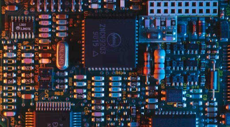
The project, led by 3D Glass Solutions, marks the introduction of cutting-edge 3D chip packaging technology in India, positioning Odisha at the forefront of next-generation semiconductor innovation.
With an estimated investment of ₹1,943 crore, the facility will have an annual production capacity of 50 million assembled units and is expected to generate around 2,500 direct and indirect jobs.
The unit is backed by major global technology players, including Intel, Lockheed Martin, and Applied Materials. The chips produced will cater to critical sectors such as aerospace, defence, artificial intelligence, and 5G technologies.
Officials noted that the project reached the groundbreaking stage within months of receiving Union Cabinet approval, underscoring its fast-track implementation.
With this development, Odisha becomes the first state in India to host both a compound semiconductor fabrication unit and an advanced 3D glass chip packaging facility, strengthening its semiconductor ecosystem.
The initiative highlights the state government’s push to attract global investments, foster high-tech industries, and build an innovation-driven economy aligned with the vision of Atmanirbhar Bharat.
Support Our Journalism
We cannot do without you.. your contribution supports unbiased journalism
IBNS is not driven by any ism- not wokeism, not racism, not skewed secularism, not hyper right-wing or left liberal ideals, nor by any hardline religious beliefs or hyper nationalism. We want to serve you good old objective news, as they are. We do not judge or preach. We let people decide for themselves. We only try to present factual and well-sourced news.
Support objective journalism for a small contribution.