


 Samsung
Samsung begins chip production using 3nm process technology with GAA architecture
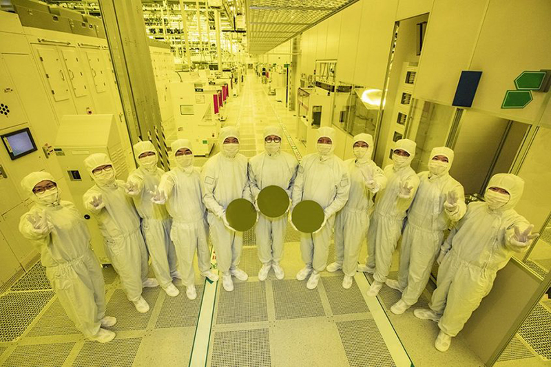
New Delhi: Samsung Electronics, the world leader in semiconductor technology, today announced that it has started initial production of its 3-nanometer (nm) process node applying Gate-All-Around (GAA) transistor architecture.
Multi-Bridge-Channel FET (MBCFET), Samsung’s GAA technology implemented for the first time ever, defies the performance limitations of FinFET, improving power efficiency by reducing the supply voltage level, while also enhancing performance by increasing drive current capability.
Samsung is starting the first application of the nanosheet transistor with semiconductor chips for high performance, low power computing application and plans to expand to mobile processors.
“Samsung has grown rapidly as we continue to demonstrate leadership in applying next-generation technologies to manufacturing, such as foundry industry’s first High-K Metal Gate, FinFET, as well as EUV. We seek to continue this leadership with the world’s first 3nm process with the MBCFET™,” said Dr. Siyoung Choi, President and Head of Foundry Business at Samsung Electronics. “We will continue active innovation in competitive technology development and build processes that help expedite achieving maturity of technology.”
Design-Technology Optimization for Maximized PPA
Samsung’s proprietary technology utilizes nanosheets with wider channels, which allow higher performance and greater energy efficiency compared to GAA technologies using nanowires with narrower channels. Utilizing the 3nm GAA technology, Samsung will be able to adjust the channel width of the nanosheet in order to optimize power usage and performance to meet various customer needs.
In addition, the design flexibility of GAA is highly advantageous for Design Technology Co-Optimization (DTCO), which helps boost Power, Performance, Area (PPA) benefits. Compared to 5nm process, the first-generation 3nm process can reduce power consumption by up to 45%, improve performance by 23% and reduce area by 16% compared to 5nm, while the second-generation 3nm process is to reduce power consumption by up to 50%, improve performance by 30% and reduce area by 35%.
Providing 3nm Design Infrastructure & Services With SAFEPartners
As technology nodes get smaller and chip performance needs grow greater, IC designers face challenges of handling tremendous amounts of data to verify complex products with more functions and tighter scaling. To meet such demands, Samsung strives to provide a more stable design environment to help reduce the time required for design, verification and sign-off process, while also boosting product reliability.
Since the third quarter of 2021, Samsung Electronics has been providing proven design infrastructure through extensive preparation with Samsung Advanced Foundry Ecosystem (SAFE™) partners including Ansys, Cadence, Siemens and Synopsys, to help customers perfect their product in a reduced period of time.
Support Our Journalism
We cannot do without you.. your contribution supports unbiased journalism
IBNS is not driven by any ism- not wokeism, not racism, not skewed secularism, not hyper right-wing or left liberal ideals, nor by any hardline religious beliefs or hyper nationalism. We want to serve you good old objective news, as they are. We do not judge or preach. We let people decide for themselves. We only try to present factual and well-sourced news.
Support objective journalism for a small contribution.