


IISc scientists propose ₹500 cr plan to develop angstrom-scale chips using 2D materials
New Delhi: A team of 30 scientists from the Indian Institute of Science (IISc) has submitted a proposal to the government to develop angstrom-scale semiconductor chips—dramatically smaller than those currently being produced worldwide.
The proposed technology is based on a new class of semiconductor materials known as 2D materials, which could pave the way for chips that are nearly one-tenth the size of the smallest chips currently in use globally.
The aim of the proposal is to leverage these advanced materials to position India as a leader in next-generation semiconductor technologies.
Chips beyond silicon: Angstrom-scale push through 2D materials
The proposed chips would be fabricated using ultra-thin materials like graphene and transition metal dichalcogenides (TMDs), classified as 2D semiconductors.
These materials are expected to enable manufacturing at the angstrom scale—far smaller than the existing nanometer technologies.
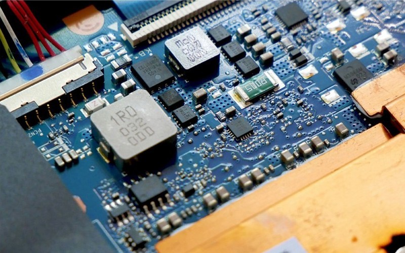
The smallest chips in current global production measure 3 nanometers and are manufactured by companies such as Samsung and MediaTek.
"A team of scientists at IISc submitted a detailed project report (DPR) to the Principal Scientific Adviser (PSA) in April 2022, which was revised and submitted again in October 2024. The report was later shared with the Ministry of Electronics and IT. The project promises to develop angstrom-scale chips, far smaller than the smallest chips in production today," a government source told PTI.
MeitY positive about the project
The Ministry of Electronics and Information Technology (MeitY) has confirmed that the proposal is under active discussion.
"MeitY is positive about the project. The Principal Scientific Adviser and Secretary, MeitY, have held meetings on it. MeitY is exploring the electronics applications where such technology can be deployed. This is a collaborative effort that requires due diligence at every step," an official familiar with the discussions said.
A brief summary of the project is also available on the website of the PSA's office.
A modest investment for a strategic leap
In contrast to India’s flagship semiconductor manufacturing initiative—Tata Electronics’ Rs 91,000 crore project with Taiwan's PSMC, which is backed by 50% capital support from the government—the IISc-led initiative seeks Rs 500 crore over five years.
The funding is intended to support foundational research and technological development, with a built-in roadmap for self-sustainability beyond the initial funding phase.
India continues to rely heavily on foreign players for chip production, a sector that is strategically significant for both economic and national security reasons.
Global race for 2D material dominance
Around the world, 2D materials are drawing significant attention and investment. Europe has allocated over USD 1 billion (around Rs 8,300 crore), South Korea has committed over USD 300 million, and other countries such as China and Japan have also made serious, though undisclosed, investments.
"2D materials will be key enablers for future heterogeneous systems. While global momentum is building, India's efforts remain limited and need urgent scaling. This is a domain where India can take leadership, but time is running out," said an officer aware of the developments.
India urged to shift from discussion to action
According to the PSA office’s website, communications on the proposal have been underway since 2021, involving outreach to several key ministries including MeitY, DRDO, and the Department of Space.
NITI Aayog recommended the project in September 2022, based on the IISc report.
An official closely following the research landscape noted that countries worldwide are preparing for a post-silicon era as traditional chip technologies approach their physical limitations.
"Global technology players have turned their attention to 2D semiconductors. India now needs to move from deliberation to execution. The proposal seeks Rs 500 crore over five years, but there is still no formal assurance. This window may not stay open for long," the official said.
Support Our Journalism
We cannot do without you.. your contribution supports unbiased journalism
IBNS is not driven by any ism- not wokeism, not racism, not skewed secularism, not hyper right-wing or left liberal ideals, nor by any hardline religious beliefs or hyper nationalism. We want to serve you good old objective news, as they are. We do not judge or preach. We let people decide for themselves. We only try to present factual and well-sourced news.
Support objective journalism for a small contribution.


