


 Semiconductor
From minerals to microchips: Odisha’s big leap into future tech
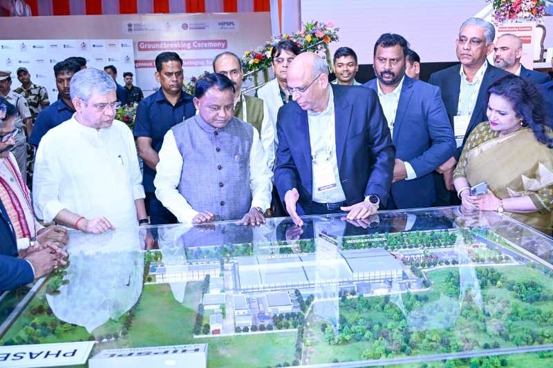
The foundation stone for India’s first advanced 3D chip packaging unit was laid on Sunday at Info Valley in Bhubaneswar, marking a major step toward strengthening the country’s semiconductor ecosystem.
The project, titled Heterogeneous Integration Packaging Solutions, is being promoted by 3D Glass Solutions and represents a significant push towards the vision of Atmanirbhar Bharat in high-end electronics manufacturing.
Project Launched with Top Leadership
The foundation stone was laid in the presence of Odisha Chief Minister Mohan Charan Majhi and Union Minister Ashwini Vaishnaw.
With this initiative, Odisha is set to host one of the world’s most advanced chip packaging technologies.
Calling it a historic milestone, Majhi said the project would bring immense pride to the state and the nation. He noted that global technology leaders such as Intel, Lockheed Martin and Applied Materials are associated with cutting-edge packaging technologies, reflecting Odisha’s growing industrial strength.
Boost to Semiconductor Ecosystem
The facility is expected to support next-generation sectors including Artificial Intelligence, high-performance computing, defence electronics, telecommunications, and advanced digital systems.
Majhi said Odisha is emerging as the only state in India hosting both the country’s first compound semiconductor fabrication unit and its first 3D glass substrate packaging facility.
The project involves an investment of nearly ₹2,000 crore and is expected to produce around 70,000 glass panels annually, along with 50 million assembled units and approximately 13,000 advanced 3DHI modules.
Employment and Growth Prospects
The Chief Minister said the growing semiconductor ecosystem would generate large-scale employment for engineering graduates, diploma holders, and ITI students, helping transform Odisha into a technology-driven growth hub.
Centre Highlights Rapid Sector Growth
Addressing the gathering, Ashwini Vaishnaw said India’s semiconductor and electronics sectors are witnessing rapid expansion, with Odisha emerging as a key contributor.
He noted that India has become the world’s second-largest mobile phone manufacturer and a leading exporter of mobile phones in 2025.
Vaishnaw added that two semiconductor projects have already been approved for Odisha under the India Semiconductor Mission, with three more proposals in the pipeline. Discussions are also underway with global firms, including Intel, for future investments.
Rail and Infrastructure Push
The Union Minister also highlighted major railway developments in Odisha, stating that projects worth over ₹90,000 crore are currently underway.
He said the state has received a record railway budget allocation of ₹10,928 crore, with 59 stations being redeveloped under the Amrit Bharat Station Scheme. Plans are also in place to connect all 30 districts through rail networks, including a proposed four-line coastal corridor from Balasore to Berhampur.
Policy Support and Future Roadmap
State Electronics & IT Minister Mukesh Mahaling said Odisha is rapidly emerging as a semiconductor hub, backed by policies on IT, AI, GCC, and semiconductors.
He highlighted initiatives such as stipend support for engineering students and upcoming events like the Blackswan Summit 2026 to boost innovation and investment.
Project Details and Timeline
The project is being implemented by 3D Glass Solutions Inc. through its Indian subsidiary Heterogeneous Integration Packaging Solutions Pvt. Ltd. at Info Valley in Khordha district.
It is a greenfield, vertically integrated advanced packaging and embedded glass substrate ATMP facility, with a total investment of ₹1,943.53 crore. This includes ₹799 crore in central fiscal support and around ₹399.5 crore from the state government.
The facility will cater to high-growth sectors such as data centres, AI, machine learning, 5G/6G communications, automotive radar, defence, aerospace, and photonics.
Commercial production is expected to begin by August 2028, with full-scale operations targeted by August 2030.
Support Our Journalism
We cannot do without you.. your contribution supports unbiased journalism
IBNS is not driven by any ism- not wokeism, not racism, not skewed secularism, not hyper right-wing or left liberal ideals, nor by any hardline religious beliefs or hyper nationalism. We want to serve you good old objective news, as they are. We do not judge or preach. We let people decide for themselves. We only try to present factual and well-sourced news.


