

 Odisha
Intel, 3DGS join hands with Odisha govt for massive advanced packaging plant, estimated investment to touch nearly USD 3.3 billion
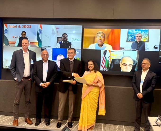
A Memorandum of Understanding (MoU) has been signed between the Government of Odisha, Intel Corporation and 3DGS Inc., USA, to establish an Advanced Packaging Glass Core Substrate Manufacturing Facility in the state.
With an estimated investment of nearly USD 3.3 billion, the project is being seen as one of the largest high-technology manufacturing investments in India. The proposed facility will be located in the Bhubaneswar-Khurda region, according to a government statement.
Union Minister for Electronics and Information Technology Ashwini Vaishnaw said the landmark MoU aligns with the Government of India’s vision of developing a complete semiconductor manufacturing ecosystem in the country.
Congratulations to the Govt. of Odisha, Intel and 3DGS on signing an MoU to bring substrate manufacturing technology to India.
— Ashwini Vaishnaw (@AshwiniVaishnaw) May 29, 2026
This will further advance semiconductor ecosystem in India. pic.twitter.com/elxs6r8muN
He noted that the entry of major global firms such as Applied Materials Inc., Lam Research, Tokyo Electron Ltd., and Merck Electronics, along with the recent agreement between Tata Electronics and Dutch semiconductor equipment giant ASML, reflects growing global confidence in India’s semiconductor ambitions.
The project is expected to be implemented in phases over the next five to six years.
Officials said the facility could generate more than 1,800 direct high-skilled jobs while also creating substantial indirect employment opportunities across the broader manufacturing and technology ecosystem.
The proposed unit will focus on advanced packaging glass core substrates, high-density interconnect substrates and related semiconductor technologies, with Intel providing technology expertise and process know-how.
The project is also expected to strengthen capability development, boost ecosystem growth and support export-oriented semiconductor manufacturing in India.
The initiative builds on the ongoing efforts under the India Semiconductor Mission to strengthen domestic manufacturing, the chip design ecosystem and supply chain capabilities. It is expected to position Odisha as one of the emerging global hubs for semiconductor manufacturing and digital infrastructure.
Support Our Journalism
We cannot do without you.. your contribution supports unbiased journalism
IBNS is not driven by any ism- not wokeism, not racism, not skewed secularism, not hyper right-wing or left liberal ideals, nor by any hardline religious beliefs or hyper nationalism. We want to serve you good old objective news, as they are. We do not judge or preach. We let people decide for themselves. We only try to present factual and well-sourced news.
Support objective journalism for a small contribution.